Training Events
Nanowiring Fall School 2013
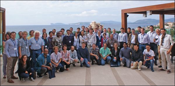
An advanced school on semiconductor nanowires covering a broad range of topics from fundamental physics to device applications was held on 6-12 October 2013 in Alghero (Sardenia, Italy)
Highly recognized international experts gave a comprehensive overview on fundamentals, recent progress and approaches to solve open questions in the exciting field of semiconductor nanowires. This advanced spring school was intended for bachelor, master and PhD students, and for post- doctorals in the field of physics, chemistry and material sciences. The purpose of the school was to draw the attention of prospective and newly graduated scientists to the latest developments in the field of semiconductor nanowires. After one day of refresher courses and tutorials on semiconductor nanostructure physics the school focused on the following topics: (1) nanowires for sensing applications, (2) nanowires for optoelectronics, (3) nanowires for nanoelectronics, (4) nanowires for energy harvesting.
Details about the programme and registration information can be found on the [Fall School 2013] website.
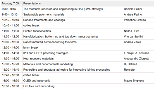
Open House Day at CRF-Fiat
The Open House Day took place at CRF-Fiat Research Center on 7. May 20112. The training event aims at providing insight on Research and Development strategies at Centro Ricerche FIAT. In particular the Nanotechnology issue in the automotive should be discussed concerning applications and Intellectual Property Rights (IPR), challenges and barriers to industrialization. The ITN fellows should get an insight into the mechanisms driving R&D in a large scale industry, also through informal exchange with representative of the Management and Human Resources.
Fellow Workshop
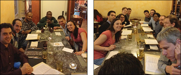
The Fellow Workshop was dedicated specifically to scientific exchange among the fellows and took place at the Politecnico Torino on 8 May 2012.
Fundamentals of Quantum Optoelectronics and Optical properties of semiconductor nanostructures
Advanced concepts and hands-on training from October 02-04, 2011 at the Cavendish Laboratory (University of Cambridge).
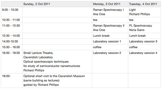
For the Laboratory sessions the group will split into two. One part will learn about aspects of Raman spectroscopy using a Jobin-Yvon T64000 triple Raman spectrometer. The other will conduct a photoluminescence experiment at 4 Kelvin on a low-dimensional semiconductor. Each of these exercises will occupy the full afternoon, so the groups will just swap over between the Monday and Tuesday sessions.