Nanowiring - Marie Curie Initial Training Network
Nanotechnology based on semiconductor nanowires promises a new generation of devices benefiting from large surface to volume ratios, small active volumes, quantum confinement effects and integration in complex architectures on the nanoscale. The main technological issues that the joint research programme intends to address within the project are the following: semiconductor nanowires for sensors, optoel-ectronic, nanoelectronic and energy harvesting applications.
 |
 |
 |
Sketch of a nanowire based single photon emitter (TU Delft) |
Rationally designed single-crystal InSb nanowire networks |
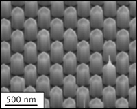
Selective area growth of GaN nanocolumns (UGOE) |
The main objective of the proposed network is to embed a pool of postgraduates and young researchers in a multidisciplinary framework of research and development activities in the emerging field of science and applications based on the unique properties and opportunities offered by semiconductor nanowires. Our mission will be to provide an excellent platform for the training of a generation that will be expected to play a leading role in developing new ideas and concepts for a truly new technology of the future. Attainment of our targets will make a substantial contribution to increased European competitiveness in one of the most important emerging technological fields.
The integration of two leading companies as full partners in the ITN underlines the strategic importance of the proposed research subject and approach. The active participation of the private sector gives additional value to the training of the early state researchers. Moreover, the synergy between partners from academia and from the private sector will contribute to expedite the research activities in Europe towards a market maturity of nanowire based applications. The project started officially on 01. November 2010 with a duration of 4 years.

